
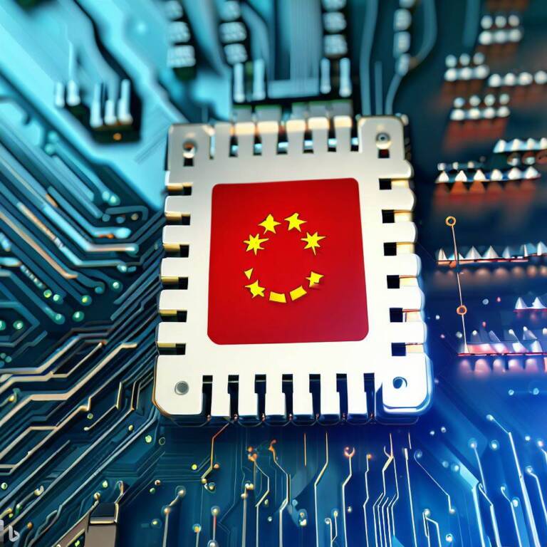
Beijing creates two-dimensional material to produce microchips. An innovation that displaces the USA
A breakthrough in the production of a new two-dimensional material , about one atom thick, is set to pave the way for the transition to next-generation semiconductors.
Chinese scientists have managed to use the new semiconductor material to produce 12-inch, approximately 36 cm wafers. This milestone could join traditional silicon chips and eventually surpass them.
The use of 2D materials in High tech is nothing new: MIT had already used 2D materials to improve the characteristics of microchips, but in this case we have a completely 2D structure and, above all, an innovation that appears ready for production industrial.
The new, extremely thin 2D material gives the wafers excellent semiconductive properties. However, before continuing with the development, the team of scientists had to solve the problems related to the scalability of the dimensions of the wafers and above all the industrialization, i.e. the possibility of producing them on a large scale.
two-dimensional materials
In an exclusive interview with the Post, Professor Liu Kaihui of Peking University, who led the project, said his team's work has ensured practical applications of the 2D material for industry. “We have demonstrated to the industry that this material is scientifically feasible and have instilled confidence. If there are industrial demands in the future, progress in this field will make great strides”.
In collaboration with Professor Liu Can of Renmin University of China and Professor Zhang Guangyu of the Chinese Academy of Sciences, his team developed the manufacturing strategy in Beijing and tested it at the Songshan Lake Materials Laboratory in Dongguan. On July 30, they published an article about their findings in the journal Science Bulletin.
While silicon is suitable for semiconductor processing, current silicon chips have faced challenges as devices continue to shrink in size.
“When silicon transistors are thinner, their voltage control gets worse. Current exists even when the device is not working. This leads to additional energy costs and heat generation,” Liu said.
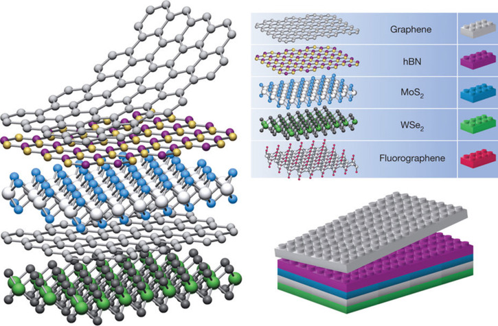
The 2D material consists of crystalline solids with one or more layers of atoms. The unique physical properties of wafers, due to their thickness naturally at the atomic level, could solve the problem. And they could find application in many high-performance electronic devices.
“Certain 2D materials are considered an essential material system for an integrated circuit of 1 nm or smaller. They are also recognized by the industry as continuing, or even exceeding, Moore's Law, which states that the number of transistors in an integrated circuit doubles approximately every two years,” the researchers say.
At each layer, 2D materials can exist separately, allowing them to be stacked layer by layer, such as graphene or transition metal dichalcogenides (TMDs), including molybdenum disulfide, tungsten disulfide, molybdenum diselenide, and diselenide of tungsten.
However, fabricating 2D material wafers with high uniformity and device performance has been a challenge for scientists worldwide. 60% of the current chip market is based on machining uniform 12-inch diameter pieces of silicon, which are the raw material from which chips are made. The difficulty was to be able to produce such a dimension of qualitatively uniform two-dimensional material and with technologies that can be replicated on a large scale, and this is the incredible result of the Chinese researchers.
This innovation will also make it possible to bypass the blocks on the export of high quality chips and components by the USA: what is the use of an imported chip if I have a much superior technology?
Biden had not considered this point.
![]()
Thanks to our Telegram channel you can stay updated on the publication of new articles from Economic Scenarios.
The article Beijing creates two-dimensional material to produce microchips. An innovation that displaces the USA comes from Scenari Economici .
This is a machine translation of a post published on Scenari Economici at the URL https://scenarieconomici.it/pechino-crea-materiale-bidimensionale-per-produrre-i-microchip-una-innovazione-che-spiazza-gli-usa/ on Mon, 28 Aug 2023 14:41:39 +0000.